Your Tech Story

Nvidia Partner SK Hynix plans to invest $4 billion in Indiana

Nvidia Partner SK Hynix Plans to Invest $4 Billion in Indiana

The massive South Korean semiconductor company and Nvidia Partner,  SK Hynix intends to build an innovative chip packaging factory in West Lafayette, Indiana, marking a significant investment in the United States. The roughly $4 billion investment is in line with the Biden administration’s objectives to increase domestic semiconductor production and is a major step towards supporting America’s semiconductor sector.

Facility Specifics and Anticipated Effect

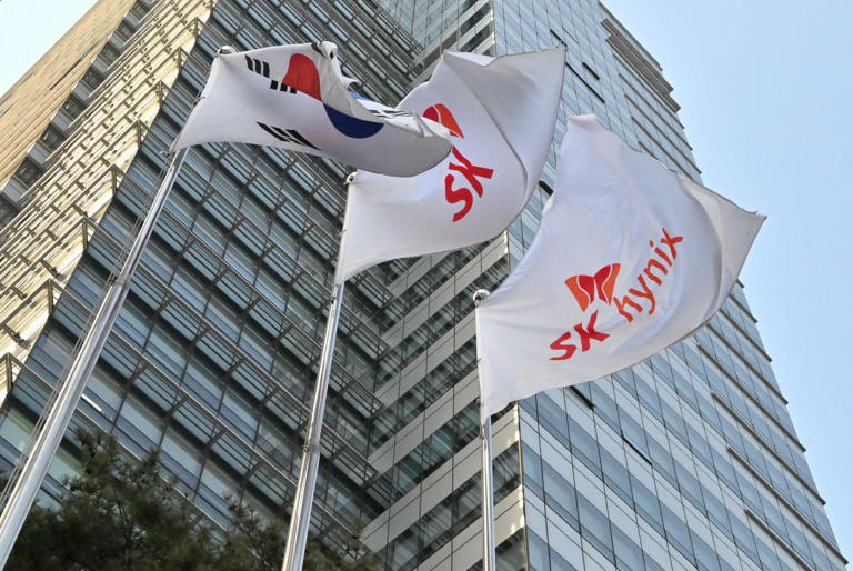
Nvidia Partner SK Hynix plans to invest $4 billion in Indiana

Image Source: msn.com

With board approval, the proposed chip packing factory is anticipated to start operations in 2028 and will likely add 800–1,000 new employees. Located near Purdue University, which is well-known for its semiconductor and microelectronics engineering programmes, the facility is ideally situated to make use of the talent and knowledge in the area.

The Market Domination of SK Hynix in Semiconductors

SK Hynix, one of the biggest chip makers in the world, has become a major force in the high-bandwidth memory (HBM) market. Because of its unique cooperation with Nvidia, SK Hynix can provide cutting-edge graphics processing units, which are essential for applications using artificial intelligence.

Investment's Significance

The SK Hynix investment serves as a reminder of the growing role that sophisticated chip packaging plays in advancing technological advancement, especially in the area of artificial intelligence. SK Hynix wants to take advantage of the rising demand for high-performance computing solutions and solidify its position in the global semiconductor industry by increasing its operations in the United States.

Consequences for the US Semiconductor Industry

The SK Hynix investment serves as a reminder of the growing role that sophisticated chip packaging plays in advancing technological advancement, especially in the area of artificial intelligence. SK Hynix wants to take advantage of the rising demand for high-performance computing solutions and solidify its position in the global semiconductor industry by increasing its operations in the United States.

Progress in the Field of Artificial Intelligence

Sophisticated methods of chip packing are essential to the advancement of artificial intelligence systems. The investment made by SK Hynix in HBM technology will further the development of AI computing by enabling quicker data processing and spurring creativity in applications that use AI.

Future Visions

SK Hynix’s entry into the American semiconductor market is indicative of an increasing trend of foreign semiconductor makers entering the market and growing their presence there. Investments in sophisticated chip packaging facilities are anticipated to increase in tandem with the emergence of AI and computational power, opening the door for more technical innovations and economic expansion.

To sum up, SK Hynix’s acquisition of the Indiana chip packing plant is a major move in the direction of expanding technological boundaries and bolstering the US semiconductor sector. Infrastructure investments in semiconductor production are positioned to spur innovation and influence the direction of artificial intelligence (AI) and other fields as consumer interest in computational power continues to increase.

Leave a Comment

Your email address will not be published. Required fields are marked *