Every decade checks the boundaries of Moore’s Law, and this decade is no exception. The complexities of multi-patterning techniques built on previous technology nodes can now be implemented with the finer resolution that EUV offers, thanks to the advent of Extreme Ultra-Violet (EUV) technology. This, along with other more technological advancements, could result in a reduction in transistor size, paving the way for the future of semiconductors. To that end, IBM announced today that it has developed the world’s first 2-nanometer node chip.
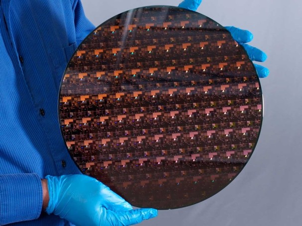
IBM 2-nm Node Chip
To be clear, though the process node is referred to as ‘2 nanometers,’ nothing about the transistor measurements resembles a conventional expectation of what 2nm would be. Previously, dimension was an analogous metric for 2D feature size on the chip, such as 90nm, 65nm, and 40nm. However, with the introduction of 3D transistor designs such as FinFETs and others, the process node name is now an interpretation of an ‘equivalent 2D transistor’ design.
Some of the features on this chip, such as transistor fin leakage safety layers, are likely to be in the low single digits in real nanometers, however, it’s crucial to remember the disconnect in how to process nodes are actually called. The debate often pivots to transistor density as a more precise measure, which IBM is sharing with us.
Density of the Transistors
According to a recent announcement, IBM’s 2nm development would boost efficiency by 45 percent at the same capacity, or 75 percent energy at the same performance, as compared to current 7nm processors. IBM is quick to point out that it was the first academic organization to demonstrate 7nm in 2015 and 5nm in 2017, the latter of which upgraded from FinFETs to nanosheet technologies that allow for greater customization of individual transistors voltage characteristics.
According to IBM, the device will fit ’50 billion transistors on a chip the size of a fingernail.’ We contacted IBM to get feedback on the scale of a fingernail since we were coming up with numbers ranging from 50 square millimeters to 250 square millimeters internally. According to IBM’s press ties, a fingernail, in this case, is 150 square millimeters. This equates to 333 million transistors per square millimeter (MTr/mm2) for IBM.
Different foundries have different official names and densities. It’s worth noting that these densities are often classified as peak densities, for transistor libraries where die area is the primary concern rather than frequency scaling – the fastest sections of a processor are often half as small as these numbers due to power and thermal considerations.
GAA Transistors
Although IBM has not expressly announced the transition to Gate-All-Around / nanosheet transistors, photographs reveal that this new 2nm processor is using a three-stack GAA architecture. GAA will be introduced by Samsung at 3nm, while TSMC will wait until 2nm. Intel, on the other hand, we believe would implement some kind of GAA on its 5nm technology.
IBM’s 3-stack GAA has a cell height of 75 nm, a cell width of 40 nm, and discrete nanosheets that are 5 nm tall and 5 nm apart. The poly pitch of the gate is 44nm, and the gate length is 12nm.
According to IBM, its design is the first to use bottom dielectric isolation channels, allowing for the 12 nm gate length, and its inner spacers are a second-generation dry process design that aids in nanosheet production. This is supplemented by the first use of EUV patterning on the FEOL sections of the process, allowing EUV at all stages of design for essential layers.
Users may be perplexed as to why we are hearing that IBM is the first to develop a 2nm chip. IBM is one of the world’s leading research centers on potential semiconductor technologies, and while not having a foundry offering of their own, IBM produces IP for their manufacturing facilities in conjunction with others.
Back in 2014, IBM sold its manufacturing to GlobalFoundries with a 10-year collaboration commitment. IBM also deals with Samsung and recently announced a partnership with Intel. No doubt, the latter two would collaborate with IBM on some level to ensure the feasibility of this new invention in their own supply chain.
The chip was developed and manufactured at IBM’s Albany testing plant, which has a 100,000-square-foot clean space. The aim of this facility is to leverage IBM’s extensive patent and licensing portfolio for partner partnerships.