Your Tech Story

microprocessor

4004 Intel Microprocessor (1)

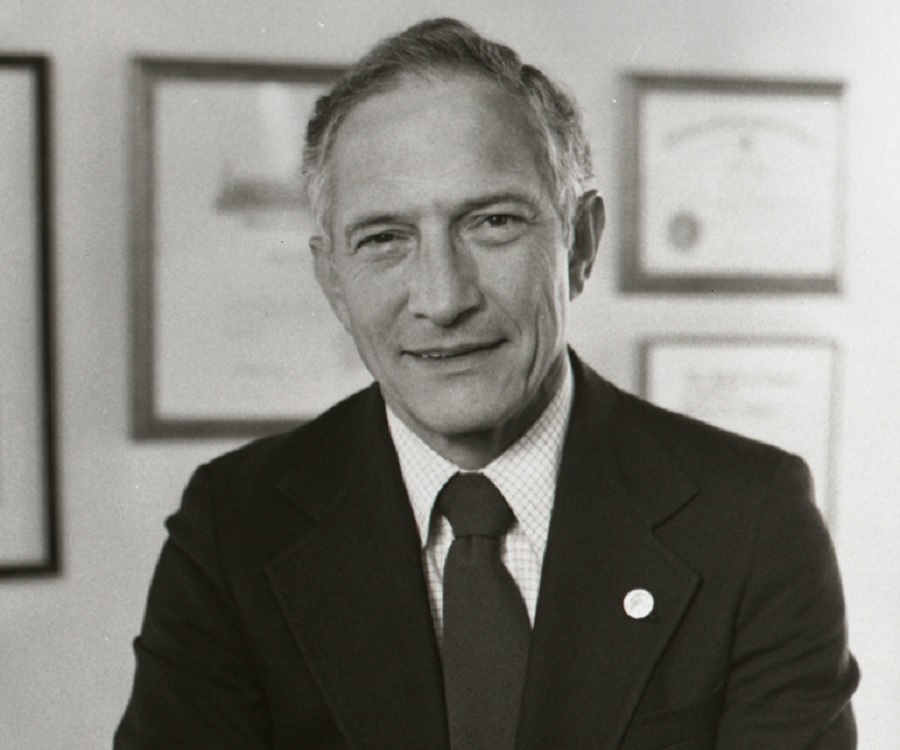
Marcian Hoff : An Electrical Engineer Who Co-invented the First Microprocessor

The modification of an already existing invention is much easier than proposing the idea of creating a new one. With time, advancement in technology and acceptance within mankind both took place, which seemed like far-fetched goals in the earlier days. Even though there were many obstacles in the past, many significant scientists emerged out on the surface with innovative innovations. And, today, these are the innovations that are helping us take a step forward towards building a smarter world.

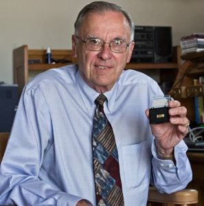
Marcian Hoff, popularly known as Ted Hoff, is one such brilliant innovator who invented microprocessor in the early 1900s. Hoff started co-invented things while he was pursuing a PhD. But, in 1968, his life completely changed its course and became a roller-coaster ride, when he was approached by Robert Noyce, co-founder of Intel Corp.

Early Life and Education of Hoff

Marcian Hoff was born on 23rd October 1937 in Rochester, New York. He was lured by the scientific world from a very young age, especially when he received a subscription to Popular Science from one of his uncles at the age of 12. For his undergraduate degree, Hoff went to Rensselaer Polytechnic Institute and graduated in 1958 with a bachelor’s degree in Electrical engineering. As an undergraduate student, he worked at Rochester’s General Railway Company during the summer breaks. During his time in this company, he worked with magnetic cores and transistors, and also developed his first two patents during this time.

Ted Hoff aka Marcian Hoff
Image Source: blog.parrikar.com

After completing his college, Hoff received a National Science Foundation Fellowship which gave him the opportunity to attend Stanford University. In 1959, he received an MS degree and a PhD from the same university in 1962. During this time, he co-invented least mean square filter with Bernard Widrow, his guide and a professor of Stanford University. The algorithm they invented is still used in modems today.

Hoff chose to stay in Stanford to carry out his studies on neural networks and integrated circuits, hence, continued research for another four years. While he was learning about integrated circuits, he realized how hard it was to build one.

During this time, Noyce was hiring for Intel, and he contacted a professor of Stanford to know if there was anyone in the campus who had the potential to become an Intel employee. And this is how Hoff ended up as Intel employee in 1968.
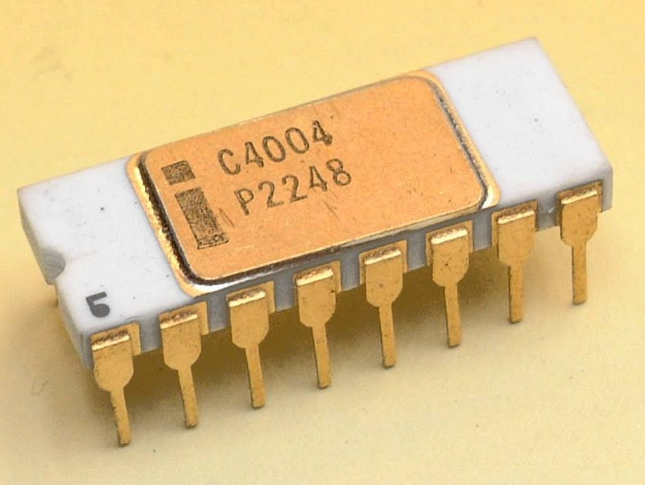
Intel 4004

Marcian Hoff joined Intel in 12th September 1968, as the company’s twelfth member. Intel was established with the main goal to replace all the magnetic core memories with semiconductor memories. Since, it totally diverted from the conventional idea about computer memory, creating a market demand was very tough. So, they decided to take up clients and develop memories as per their requirements. Intel’s first customer for this semiconductor memory was a Japanese company who sold calculators under the name Busicom.

They demanded different types of chips for performing various activities, and hence, both the companies signed a contract to create these chips in April 1969. After this contract, engineers were sent from Japan to work on this design, but at the same time, Hoff on behalf of Intel created another design, which used DRAM (dynamic random access memory). The company liked Intel’s approach better, as a lesser number of chips were able to perform more functions.

Intel, after successfully designing product for this client, wanted to expand the utility of silicon gate, and they hired Dr Faggin in April 1970 to conduct research and make progress on this area. Today, this metal oxide silicon (MOS) process is extensively used in what we call embedded system.

Hoff said that nobody in the company expected as much growth as took place in the following years.

What after Intel 4004 project?

After the 4004 project, Noyce’s next target was to implement their MOS technology in telephony. So, Hoff started working CODEC (a decoder working used in the telephonic industry to convert analog signals to digital and vice versa). Intel was able to come up with monolithic CODEC which could be used commercially.

Hoff left Intel in 1983 and joined Atari as it was working on some really advanced ideas. But, the business strategies of the company were very poor, which resulted in the dropping of the revenue from $2 billion to $1 billion within a single year. Hoff left Atari in 1985 when the company was sold.

From Engineering to understanding Business

Today, Hoff is the part of Teklicon, a company that deals with business and law; established by Gary Summers, who was the head of semiconductor designing in Atari, when Hoff joined the company.

Intel’s 9th Gen Core i9 9900K; The Fastest Gaming Processor Ever

Intel
Image Source: techcarving.com

Intel, the 800-pound gorilla of the processor world, is back with a substantially higher clock speedCore X microprocessors lineup, including the $263 Core i5-9600K, the $385 Core i7-9700K and the $499 Core i9-9900K. The new processor chip is high at performance, providing new levels for the power users and the gamers. The chips are considerably powerful than the AMD’s Ryzen 7 2700X, and the Core i9-9900K is the fastest of them all.

The Coffee Lake architecture based processor has the Base Frequency (GHz) of 3.6, and the Boost Frequency (Active Cores – GHz) of 1-2 Cores – 5.0, 4 Cores – 4.8, and 8 Cores – 4.7. It is using the Solder Thermal Interface Material (STIM), to facilitate the better thermal transfer, on the Core i9 and i7 models without disrupting a 95W cover at base clock rates. The processor has the eight Hyper-Threaded cores (8C/16T) and comes with better frame rates.

The Core i9-9900K has been manufactured on the Intel’s 14nm++ node and supports the dual-channel DDR4-2666 memory. The chip is integrated with the UHD 630 graphics engine and provides with the facility to double the memory capacity support to increase the RAM density up to 128 GB. It consists of the Dual-Channel Memory Controller and x16 PCIe Lanes. The processor is accompanied by two additional 2MB slices of L3 cache.

The processor is considered to be providing the best performance than its contemporaries, especially to play games on the 4K or HDR. But, the extra frames offered with it are not making much of the difference comparing to the 8th Gen processor, and are not worth spending this much money. The chip has introduced various features against its competitor AMD, but still the processor is at a higher price.

Qualcomm Unveils Snapdragon 675 Processor Supporting Tripple Camera & Advanced AI

Qualcomm, best known for its next-generation mobile technologies and powerful Snapdragon processors, has just launched the new Snapdragon 675, the latest high to the mid-range mobile computing platform. The production of the Snapdragon 625 is basically focussed on the better gaming experience, photography, and artificial intelligence (AI).

The Snapdragon 625 is being considered as an upgrade over the Snapdragon 670 SoC that was launched in August this year. The Snapdragon 625 chipset has the Kryo 460 architecture that is built on the ARM’s Cortex-A76 cores. The architecture is specially designed for high-end smartphones. It is the first time that the processor has been manufactured using the 11nm process. The processor has got two 2.0GHz performance cores, four 2.8GHz performance cores that are based on the Cortex-A75, and six 1.78GHz efficiency-based cores, making the processor faster.

SND
Image Source: droidsans.com

With Snapdragon 625, Qualcomm has brought the features, that were only available for high-end smartphones, to the mid-range smartphones. Snapdragon 625 has got a new Qualcomm Spectra 250L ISP for 14-bit image signal processing supporting a triple-camera setup, with 5x optical zoom, 48 megapixels, portrait mode, etc.

The processor is also focussed on improving the gaming experience and the AI features. According to the company, the AI features have been improved by 50% than the previous processors, with the help of third-generation Qualcomm AI Engine. The processor supports the Qualcomm Neural Processing Engine SDK, resulting in the addition of features like the adaption of user’s voice, working with multiple voice assistants, etc.

Also, the processor has faster performance, supporting high-end games like PUBG, Best NBA, Honor of Kings, Knives Out, etc. The processor uses the Adreno 612 GPU that supports OpenGL ES 3.2, Open CL 2.0, Vulkan, and DirectX 12. Snapdragon X12 LTE modem supports up to 600Mbps LTE connectivity that provides a support for playing the online games without any interruption.

The Qualcomm’s Snapdragon chipset is used in every other smartphone. The Snapdragon 625 can be considered Qualcomm’s attempt to provide the users of mid-range smartphones a better experience with its high-end features. By the first quarter of next year, you can find the Snapdragon 625 processors out in new Smartphones.

Robert Noyce : Co-Founder of Intel & Co-Inventor of the Integrated Circuit

A scuba diver, a pilot, an inventor and what not? Known as the Mayor of the Silicon Valley, the legendary inventor Robert Noyce made his mark in the history of Semiconductors. Noyce was a sharp student and had shown his traits as an inventor, from his childhood. From building a boy-sized aircraft to creating a transistor from scratch, he always loved playing with machines. Having a sharp mind, he also gained the name Rapid Robert from his classmates. This remarkable physicist had brought a revolution in the field of personal computers with its the first integrated circuit and gave Silicon Valley its name.

Early Life

Robert was born to Rev. Ralph Brewster Noyce and Harriet May Norton, on 12 December 1927, in Burlington, Iowa. He was the third of his three siblings, Donald Sterling Noyce, Gaylord Brewster Noyce and Ralph Harold Noyce. Noyce was a brilliant student, and was also, good at other co-curricular activities like sports, acting and singing. He completed his high school from Grinnell High School and enrolled himself into the physics course in Grinnell College. During his school days, he excelled in mathematics. Later, he joined MIT and received a PhD in solid-state physics in 1953.

Early Career

During his PhD, Noyce found his interest in transistors. After the completion of his PhD, he joined Philco Corporation in Philadelphia as the research engineer. In 1956, he left the job at Philco and joined the Shockley Semiconductor Laboratory in Mountain View, California, owned by the co-inventor of transistor and Nobel prize winner, William Shockley. He worked there for a year and left the company with the infamous ‘traitorous eight’ on having a dispute with William Shockley, on his way of working.

Founding Intel

After quitting the Shockley Semiconductor Laboratory, he co-founded a semiconductor company named Fairchild Semiconductor, with Sherman Fairchild, the owner of Fairchild Camera and Instrument, in 1957. At Fairchild Semiconductor, Noyce co-invented the first Integrated Circuit built with Silicon. During the invention of this IC, he also developed a planar process, that made it easy to develop the transistors at a lower cost.

Robert Noyce
Image Source: thefamouspeople.com

Working for 9-long years, Noyce left the Fairchild Semiconductors and co-founded NM Electronics, with his former co-worker, Gordon Moore, from Shockley Semiconductor Labs, in 1968. Later, NM Electronics was renamed to Intel Corporation. Noyce served as the President of Intel till 1975 and in 1978, chaired the board of directors of Intel, till 1978.

The team intel invented the first commercially successful product, the 3101 Schottky bipolar 64-bit static random access memory (SRAM) chip, in May 1969. In 1971, Intel made the first single-chip microprocessor in the world, that made Intel more famous, that ignited the personal computer revolution.

Noyce was popular for his working style and employee administration, that was the main reason of his leaving the Shockley Semiconductor Labs. He provided the employees with rewards and bonuses to encourage teamwork. He created a relaxed working environment for the employees, and avoided any type of luxuries, to maintain equality among every employee.

In 1978, he left Intel and joined the Semiconductor Industry Association (SIA) as the chairman. In 1988, Noyce decided to get retired and established an association named SEMATECH, a semiconductor manufacturing consortium with the help of SIA and held the position of the President of the company.

Personal Life and Death

Noyce married Elizabeth Bottomley in 1953 and had four children with her. The two got divorced in 1974. Noyce on 27 November 1974, got married to Ann Schmaltz Bowers, who became the first Director of Personnel for Intel Corporation.

On 3 June 1990, Noyce died of heart attack, at the age of 62.

In his life, Noyce kept himself busy in various inventions and got his name recorded as a great inventor. He received many awards for his contribution to the technology, including the Stuart Ballantine Medal in 1966, IEEE Medal of Honor in 1978, National Medal of Science in 1979 and National Medal of Technology in 1987.