Sony launches IMX661 127.68 Megapixel Image Sensor with Global Shutter Function
This week Sony has broken big news for the launch of a large-format CMOS Image Sensor that will come with a global shutter function. Sony has revealed the specifications and features of the product and the name of this image sensor is IMX661. According to Sony, the newly released image sensor has the highest effective pixel count in the entire industry. It is one of its first kind and the product will be starting to ship from April of this year.
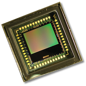
Sony IMX661 Image Sensor
Sony IMX661 has the highest effective pixel count of 127.68 megapixels and this sensor will provide nearly 10 times larger optical sizes than a typical 1.1-type image sensor (Gadgets 360). The new image sensor is developed based on Sony’s Pregius technology. Pregius is defined as Sony’s global shutter pixel technology which is further based on Sony’s low-noise CCD structure.
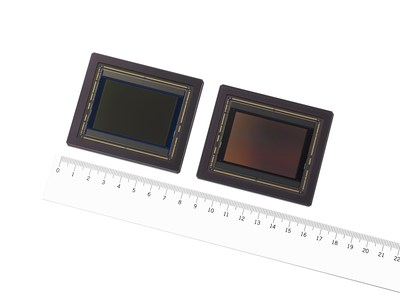
(left: color model, right: black and white model)
Image Source: sony.com
The company claims that one of the best features of IMX661 is that it can capture moving objects much more effectively without causing distortion. Sony image sensor is designed in such a way that it is capable of four times faster image readout speeds as compared to any other typical CMOS image sensor. So, let’s have a detailed look at all the specifications and features of the Sony IMX661 image.
Major Improvements
The advent of the digital era and especially the AI revolution has increased the demand for CMOS image sensors exponentially. Today, in various fields across any industry, image sensors are of much importance as a part of industrial equipment. Sony via its newly launched IMX661 aims to solve many complicated challenges across many industries where image sensors are of much importance.
The new image sensor is a combination of Sony’s Pregius technology along with a 3.6-type large optical size. These are the two main technologies when combined together will deliver a high pixel count and distortion-free images of moving objects. The image sensor also captures highly efficient images using a wide viewing angle along with no motion distortion in a single operation.
Sony IMX661 delivers a high level of performance in terms of image processing and this image sensor also has improved precision for recognition. So, in the fields of crime detection, Sony IMX661 will help hugely in facial recognition with a plus point of the distortion-free image. Not to mention that Sony IMX661 is a boon for all wildlife photographers out there for whom one of the most important things is capturing moving subjects sharply.
Specifications of Sony IMX661
Sony IMX661 will be available in two colors, namely, black and white. The unit cell size of the product is 3.45 X 3.45 micrometer. This large-format CMOS image sensor has a diagonal optical size of 56.73mm. Sony said the sensor is the best option for using in wide-area monitoring and aerial photography. This brings us to one of the most important features of this image sensor, i.e., high resolution with extreme precision images.
Sony IMX661 is also rolling out with improved image readout speed to offset the increased signal processing volume (Gadgets 360). The new sensor is capable of delivering a frame rate of 12.9 fps for 14 bit, 19.6 fps for 12 bit, and 21.8 fps for 10 bit. Sony IMX661 also has improved AD converter processing functionality without increasing the product size. This is mainly due to Sony’s original configuration of the chip-on-wafer process.
To make the output interface faster, Sony has also embedded Scalable Low Voltage Signaling with Embedded Clock which has comparatively high-speed interface standards. Some of the other included features in the Sony IMX661 that are especially helpful in industrial equipment include trigger synchronization, Region of Interest (RoI) gradation compression, multi-exposure, pixel binning readout, etc.
Availability of Sony IMX661
Though the company is launching the IMX661 image sensor for industrial equipment, Sony might embed the high pixel count feature in consumer products as well. The product will start shipping in April 2021. The basic colors of the model will be either black or white, specifications of other colors are not provided in detail yet.

Annasha Dey is an NIT student, who apart from studying engineering is also a content writer. She has a great interest in photography, writing, reading novels, and travelling as well. She is a foodie who loves socializing and hanging out with her friends. She is also a trained Kathak dancer and a big fashion enthusiast. Dey also loves watching TV series, which includes F.R.I.E.N.D.S. and Big Bang Theory. To be a better writer she prefers to read more